?2011 Fairchild Semiconductor Corporation
www.fairchildsemi.com
FAN4800AU/CU " Rev. 1.0.1
5
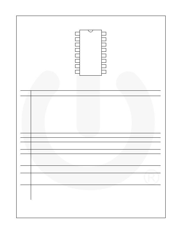
Pin Configuration
IE A
R A M P
R T / C T
F B P W M
S S
V R M S
I S E N S E
I A C
I L I M I T
G N D
O P W M
O P F C
V D D
V R E F
F B P F C
V E A
1
2
3
4
5
6
7
8
1 6
1 5
1 4
1 3
1 2
1 1
1 0
9
Figure 6. Pin Configuration (Top View)
Pin Definitions
Pin # Name
Description
1
IEA
Output of PFC Current Amplifier. The signal from this pin is compared with an internal
sawtooth to determine the pulse width for the PFC gate drive.
2
IAC
Input AC Current. For normal operation, this input provides a current reference for the
multiplier. The suggested maximum I
AC
is 65 礎.
3
ISENSE
PFC Current Sense. The inverting input of the PFC current amplifier and the output of
multiplier and PFC I
LIMIT
comparator.
4
VRMS Line-Voltage Detection. The pin is used for the PFC multiplier.
5
SS
PWM Soft-Start. During startup, the SS pin charges an external capacitor with a 10 ?/SPAN>A
constant current source. The voltage on FBPWM is clamped by SS during startup. If a
protection condition occurs and/or PWM is disabled, the SS pin is quickly discharged.
6
FBPWM PWM Feedback Input. The control input for voltage-loop feedback of PWM stage.
7
RT/CT Oscillator RC Timing Connection. Oscillator timing node; timing set by R
T
and C
T
.
8
RAMP
PWM RAMP Input. In Current Mode, this pin functions as the current-sense input. In Voltage
Mode, it is the feed-forward sense input from PFC output 380 V (feed-forward ramp).
9
ILIMIT Peak Current Limit Setting for PWM. The peak current limit setting for PWM.
10
GND
Ground
11
OPWM
PWM Gate Drive. The totem-pole output drive for the PWM MOSFET. This pin is internally
clamped under 19 V to protect the MOSFET.
12
OPFC
PFC Gate Drive. The totem-pole output drive for PFC MOSFET. This pin is internally clamped
under 15 V to protect the MOSFET.
13
VDD
Supply. The power supply pin. The threshold voltages for startup and turn-off are 11 V and
9.3 V, respectively. The operating current is lower than 10 mA.
14
VREF
Reference Voltage. Buffered output for the internal 7.5 V reference.
15
FBPFC
Voltage Feedback Input for PFC. The feedback input for PFC voltage loop. The inverting input
of PFC error amplifier. This pin is connected to the PFC output through a divider network.
16
VEA
Output of PFC Voltage Amplifier. The error amplifier output for PFC voltage feedback loop.
A compensation network is connected between this pin and ground.
发布紧急采购,3分钟左右您将得到回复。
相关PDF资料
FAN4800CUN
IC PWM/PFC CTLR COMBO 16-MDIP
FAN4802MY
IC PFC CTRLR AVERAGE CURR 16SOP
FAN4802SNY
IC CTLR PFC/PWM COMBO 16-PDIP
FAN6920MRMY
IC PWM CTLR PFC/QUASI-RES 16SOP
FAN6921MLMY
IC CTLR PFC/FLYBACK 16-SOICN
FAN6921MRMY
IC CTLR PFC/FLYBACK 16-SOICN
FAN6961SZ
IC PFC CONTROLLER DCM 8SOP
FAN6982MY
IC CTLR PFC CCM 14-SOICN
相关代理商/技术参数
FAN4800C
制造商:FAIRCHILD 制造商全称:Fairchild Semiconductor 功能描述:PFC/PWM Controller Combination
FAN4800CMY
功能描述:电流型 PWM 控制器 PWM/PFC, Avg Curr 30uA SU, 2.6mA Op RoHS:否 制造商:Texas Instruments 开关频率:27 KHz 上升时间: 下降时间: 工作电源电压:6 V to 15 V 工作电源电流:1.5 mA 输出端数量:1 最大工作温度:+ 105 C 安装风格:SMD/SMT 封装 / 箱体:TSSOP-14
FAN4800CNY
功能描述:电流型 PWM 控制器 PWM/PFC, Avg Curr 30uA SU, 2.6mA Op RoHS:否 制造商:Texas Instruments 开关频率:27 KHz 上升时间: 下降时间: 工作电源电压:6 V to 15 V 工作电源电流:1.5 mA 输出端数量:1 最大工作温度:+ 105 C 安装风格:SMD/SMT 封装 / 箱体:TSSOP-14
FAN4800CS
制造商:FAIRCHILD 制造商全称:Fairchild Semiconductor 功能描述:PFC/PWM Controller Combination
FAN4800CSMY
功能描述:电流型 PWM 控制器 PFC/PWM Controller Combination RoHS:否 制造商:Texas Instruments 开关频率:27 KHz 上升时间: 下降时间: 工作电源电压:6 V to 15 V 工作电源电流:1.5 mA 输出端数量:1 最大工作温度:+ 105 C 安装风格:SMD/SMT 封装 / 箱体:TSSOP-14
FAN4800CSNY
功能描述:电流型 PWM 控制器 PFC/PWM Controller Combination RoHS:否 制造商:Texas Instruments 开关频率:27 KHz 上升时间: 下降时间: 工作电源电压:6 V to 15 V 工作电源电流:1.5 mA 输出端数量:1 最大工作温度:+ 105 C 安装风格:SMD/SMT 封装 / 箱体:TSSOP-14
FAN4800CUM
功能描述:电流型 PWM 控制器 PFC/PWM Controller Combination RoHS:否 制造商:Texas Instruments 开关频率:27 KHz 上升时间: 下降时间: 工作电源电压:6 V to 15 V 工作电源电流:1.5 mA 输出端数量:1 最大工作温度:+ 105 C 安装风格:SMD/SMT 封装 / 箱体:TSSOP-14
FAN4800CUN
功能描述:电流型 PWM 控制器 PFC/PWM Controller Combination RoHS:否 制造商:Texas Instruments 开关频率:27 KHz 上升时间: 下降时间: 工作电源电压:6 V to 15 V 工作电源电流:1.5 mA 输出端数量:1 最大工作温度:+ 105 C 安装风格:SMD/SMT 封装 / 箱体:TSSOP-14
